Article citation information:
Breus, A., Pavlenko, V. Effect
of impulse bias potential on formation of wearproof coating
deposited by plasma fluxes. Scientific
Journal of Silesian University of Technology. Series Transport. 2016, 92, 17-22. ISSN: 0209-3324. DOI: 10.20858/sjsutst.2016.92.2.
Andrey BREUS[1], Vitaliy PAVLENKO[2]
EFFECT OF IMPULSE BIAS
POTENTIAL TO FORMATION OF WEAR-PROOF COATING DEPOSITED FROM PLASMA FLUXES
Summary. Plasma-based technology is used to deposit a
wear-proof nanostructured coating on plunger tappets
of pump of aviation oil system block, which allows increasing the life of the
parts up to 3–5 times. For the nanostructured coatings, which are formed
at the impulse bias supply, the electric field strength is 103-104
times greater than for the microstructured coatings. It
results in significant change of activation energy of the process of strong
bond formation in the growing coating, which makes it possible to obtain high
qualitative characteristics of the coating.
Keywords: plasma-based deposition; nanostructured coatings; impulse bias
1. INTRODUCTION
Nowadays
new technologies and materials are widely applied for transport quality
improvement and increasing of its service life [1]. Ion-plasma technologies
have been used for the last 50 years to change the surface properties for various
applications [2-5]. The method of plasma immersed ion implantation and
deposition (PIII&D) has become especially widespread [6, 7]. The essence of
this method is that the work piece, located on the substrate,
is under negative potential, which makes it possible to accelerate the ions in
the electrostatic layer, which is formed between the work piece and
plasma. The energy supplied by ions to the growing coating, allows activating a
range of processes, simultaneously avoiding the significant increase of the
work piece temperature. When the coating is deposited without plasma and
PIII&D method, the typical temperature of the work piece should reach
the value of more than 0.6Tm
(where Tm is melting
temperature) to obtain the coating with proper characteristics. PIII&D
methods allow increasing the work piece temperature only to the value of about
0.4Tm, which make it
possible to prevent recrystallization and loss of positive characteristics
obtained at preliminary heat treatment. However, the temperature of 0.4Tm allows obtaining microstructured coatings, thus limiting the work piece
service properties. To overcome this limit, a transition from “traditional” microstructured coatings to nanostructured coatings with
grain size of about 10-9 m should occur. The temperature should be
lowered to the values of about (0.2…0.3)Tm to obtain such coatings; a big number of
crystallization grains appears at such condition, which facilitates the formation
of fine-grained structure. However, the speed of strong bonds formation is very
low in the coating due to the low temperature; the mechanical characteristics
of obtained coatings are not adequate because of big number of pores.
To
obtain nanostructured coatings we can apply the impulse high negative potential
to the substrate coupled with the background constant (floating) negative
potential. We used the technique to deposit wear-proof coating to the plunger tappets of pump of aviation oil system
block, and the life of the part was increased up to 3–5 times comparing to the
un-treated samples. Microscopic investigation shown that a nanostructured
coating is formed under the influence of the impulse bias supply. The purpose
of this paper is to describe the possible mechanism of coating formation
under such conditions.
2. EXPERIMENTAL RESULTS
The experimental setup is shown
schematically in Fig. 1 (left); the work pieces are shown in Fig. 1
(right).
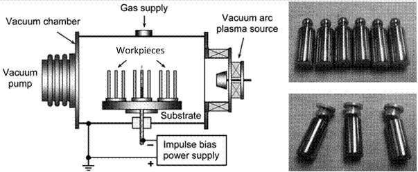
Fig. 1. Experimental setup and work pieces
The setup includes vacuum chamber
with a vacuum arc plasma source mounted on a flange of the chamber. An
evaporated cathode was made of titanium. A rotating substrate with fixtures for
work pieces installation was located in the chamber. When operating the plasma
source, the dc arc current was applied between the cathode and the grounded walls
of the vacuum chamber, which served as anode. A source of impulse bias
(2 kV, 1 µs, 1 kHz) was used to supply power
to the substrate. An automated gas-handling system maintained a nitrogen
pressure of 0.1 Pa. The time of the work pieces
exposure to the plasma was 20 min. TiN coatings with columnar structure with diameter
of about 30 nm and microhardness of 20 GPa were obtained on the surfaces
of the work pieces as a result of the plasma treatment; the temperature of the
samples did not exceed 450 K at the experiment. The coatings with the diameter
of the columnar structure of about 200–400 nm and the same microhardness can be obtained at constant bias potential of
100 V and the temperature of the samples of 750 K, which is not allowed by
the specifications for the work pieces. To describe the experimental results,
the following theoretical model was developed.
3. THEORETICAL MODEL
The model is based on
the fact that electrical field strength is higher in those areas of conductor
where the radius of curvature is smaller. We apply the known assumptions [8] to
the model, when the grain of the growing coating with radius Rnano
rests on the grain of the substrate (work piece) with radius of Rmicro.
The electrostatic potential can be calculated by use of formula for spherical
charge qi:
![]() . (1)
. (1)
For charges
equilibrium we need the equality of potentials jnano = jmicro, which results
in:
![]() . (2)
. (2)
Since the field at
the outer surface of the conductor is:
![]() , (3)
, (3)
where s is the local surface charge density, which is
proportional to the total charge divided by radius squared, we can state that:
![]() . (4)
. (4)
The ratio between the
strength Еmicro and the value of the bias potential Us applied to the substrate
can be determined by use of the cathode layer thickness s:
![]() (5)
(5)
![]() . (6)
. (6)
The presence of
electric field on the grain surface results in changing the rate of formation
of strong bonds between the deposited ions and grains of coating on the
substrate surface. This rate is proportional to the probability described by
factor exp(-ea/kT), where ea is the energy
of bond formation, T is the substrate
temperature [9]. Considering the influence of the additional electric field to
the probability of the strong bond formation, we can write:
![]() (7)
(7)
where Deа is the work, carried
out by electric field Еnano to
overcome the repulsive force between the ion and the grain at the distance of
around lattice parameter a0:
![]() (8)
(8)
Then finally, we can write:
 . (9)
. (9)
High negative
potential supplied to the grain surface, results in generation of strong
electric field, which can reduce significantly the activation energy of the
process of strong bond formation according to formula (9), thus compensating low
temperature T of the growing surface.
The need to supply
the high potential at specifically pulse mode is conditioned by two
constraints. The first is the requirement to sustain a relatively low
temperature of the work piece thus lowering the heat current supplied by ions
to the substrate after acceleration in the cathode layer. The second
constraint is imposed by the rate of change of work piece geometry, which
becomes negative (the work piece coating and surface layer are predominantly sputtered),
when the energy of ions exceeds the value of approximately 500 eV. Hence,
to deposit a wear-proof coating at low temperatures, we need to supply the high
impulse negative potential, when the ratio of the impulse duration to the impulse
period is significantly smaller than one.
To justify the proposed
mechanism of influence of the impulse bias supply to the substrate at the coating
growth, we calculated the probability Pa(Us, Rnano, T) of the strong bond formation of the
system “nanostructured coating – microstructured work
piece” with respect to the probability Pa(0, Rmicro, T) of the strong bond formation of the
system “microstructured coating – microstructured
work piece”.
Fig. 2a shows the
results of calculations of electric field strength on the surface of a grain of
a coating at dependence on the grain radius
Rnano, when the radius of the grain of
the substrate material is Rmicro = 10 µm. The amplitude of
the impulse bias of Us = 2000 V
and the plasma sheath thickness of s = 0.1 mm
are considered as parameters. Then we considered the growth of a nano-sized grain of a coating with radius of Rnano = 50 nm
on a surface of a micro-sized grain of substrate with radius of Rmicro = 10 µm.
The results of calculation of ratio Pa(2000 V, 50 nm, 450 K)/Pa(0, 10 µm, 750 K)
are shown in Fig. 2b. These results allows comparing the growth of the
wear-proof coating when the substrate temperature is low (T = 450 K) but high bias potential is supplied (Us = 2000 V) which
corresponds to conditions in our experiment, with the deposition of the
wear-proof coating when the substrate temperature is high (T = 750 K) and the bias potential is not supplied (Us = 0) that is
close to a conventional process of growth in plasma.
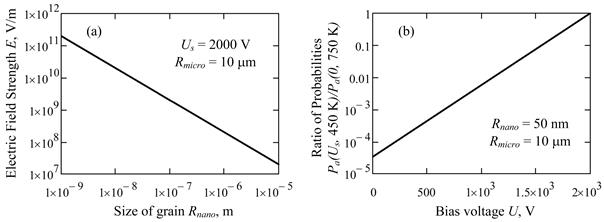
Fig. 2. Electric field strength E at dependence on radius Rnano
of a grain of coating at interaction with a grain of work piece (substrate) of radius
Rnano = 10 µm (a), and ratio of probabilities Pa(2000 V, 50 nm, 450 K)/Pa(0, 10 µm, 750 K)
at dependence on voltage U (b)
According to the calculations, the electric field strength for the
nanostructured coatings exceeds 103-104 times the
strength obtained for microstructured coatings, when
the impulse of high bias potential is applied to the substrate. At the
potential of 2000 V and coating with grain sizes of 50 nm deposited
on the surface with grain size of 10 µm, the probability Pa(2000 V, 50 nm, 450 K)
of strong bonds formation at the substrate
temperature of 450 K equals the probability Pa(0, 10 µm, 750 K) of strong bonds formation at the substrate temperature of 750 K.
Thus, impulses of high negative potential allows changing significantly the
activation energy of the process of strong bonds formation in the growing
coating, which makes it possible to obtain high quality characteristics of
coating at growth temperature of about 450 K.
4. CONCLUSION
The developed
model allows describing adequately the effect of high negative impulse potential
applied to the substrate for deposition of wear-proof nanostructured coating.
The model can be useful to describe the changes in quality characteristics
of a surface layer, which depend on bonding energy between the atoms of growing
coating such as microhardness, adhesion, inherent
stress, reflecting power, friction factor, durability, etc.
References
1.
Posmyk Andrzej. 2012. “Wpływ
nowych technologii i materiałów na poprawę jakości
transportu”. [In Polish:
“Acting of new technologies and materials on transport quality improvement”]. Scientific Journal of Silesian University of
Technology. Series Transport 78: 133-138. ISSN 0209-3324.
2.
Chen
Francis, Jane Chang. 2003. Lecture notes on principles of plasma
processing. New York: Plenum/Kluwer Publishers. ISBN 978-0-306-47497-2.
3.
Keidar Michael, Alex Shashurin, Olga Volotskova, Mary
Ann Stepp, Priya
Srinivasan, Anthony Sandler, Barry Trink. 2013. “Cold
atmospheric plasma in cancer therapy”. Physics of Plasmas 20. ISSN
1089-7674. DOI: 10.1063/1.4801516.
4.
Mariotti Davide,
R. Mohan Sankaran. 2011. “Perspectives on atmospheric-pressure plasmas for nanofabrication”. Journal of Physics D: Applied Physics
44.
ISSN 0022-3727. DOI: 10.1088/0022-3727/44/17/174023.
5.
Martina Filomeno, Jorn Mehnen, Stewart W. Williams, Paul Colegrove,
Frank Wang. 2012. “Investigation of
the benefits of plasma deposition for the additive layer manufacture of Ti-6Al-4V”. Materials
Processing Technology 212: 1377-1386.
ISSN 0924-0136. DOI: 10.1016/j.jmatprotec.2012.02.002.
6.
Metel Alexander. 2002. “Plasma immersion ion implantation based on glow discharge with
electrostatic confinement of electrons”. Surface
and Coatings Technology 156:
38-43. ISSN 0257-8972. DOI: 10.1016/S0257-8972(02)00070-1.
7.
Lieberman Michael,
Allan Lichtenberg. 2005. Principles of plasma discharges for materials
processing. New York: Wiley InterScience. ISBN
978-0-471-72001-0.
8.
Feynman Richard,
Robert Leighton, Matthew Sands. 1963. The
Feynman Lectures on Physics. Boston, MA: Addison-Wesley Co. ISBN 0-201-02115-3.
9.
Kittel
Charles, Herbert Kroemer. 1980. Thermal
Physics. New York: W.H. Freeman and Co. ISBN
978-0716710882.
Received 15.01.2016;
accepted in revised form 25.07.2016
![]()
Scientific Journal of Silesian University of
Technology. Series Transport is licensed under a Creative Commons Attribution
4.0 International License